4 Segment Back Scattered Electron Detector - Because of this, the detector can only collect secondary electrons from the thin top layer of a in contrast, backscattered electrons are formed from elastic scattering events.
4 Segment Back Scattered Electron Detector - Because of this, the detector can only collect secondary electrons from the thin top layer of a in contrast, backscattered electrons are formed from elastic scattering events.. •elastically scattered— no energy loss, large scattering angle. Backscattered electron detector — addition and subtraction is allowed. Coulomb interaction with the electron cloud • high angle scattering, or back backscattered electrons bse. Atomic weight backscattered electron detector backscattered electron imaging contrast weight fraction for element i in a. Electron detector and image reconstruction.
To obtain shadow image, the. Inner segment (preferentially compositional contrast) and electrons. The thickness of electron transparent samples can be measured in an electron microscope using several imaging techniques like electron energy loss spectroscopy. Scattering cross sections are calculated @inproceedings{gassner2011proposedse, title={proposed scattered electron detector system as one of the beam overlap diagnostic tools. Introduction to electron back scatter diffractio by prof shashank shekhar, iit kanpur.
Back scattering electron - back-scattered electron imaging ... from fosahad.info • no energy transfer • low angle scattering: Were sectioned into 1 mm thick segments with a high speed diamond saw. To obtain shadow image, the. •elastically scattered— no energy loss, large scattering angle. Secondary or backscattered electrons leaving the sample after interaction with the incident electron beam when a beam of free electrons impinges on a fiber, there are two likely outcomes, as shown in fig. Both backscattered electrons (bse) and second electrons (se) are generated when a primary beam interacts with a sample. Atomic weight backscattered electron detector backscattered electron imaging contrast weight fraction for element i in a. The thickness of electron transparent samples can be measured in an electron microscope using several imaging techniques like electron energy loss spectroscopy.
Interaction of an accelerated electron beam with a sample target produces a variety of elastic and inelastic collisions between electrons and atoms within the sample.
Both backscattered electrons (bse) and second electrons (se) are generated when a primary beam interacts with a sample. » although secondary electron imaging is the most popular. •elastically scattered— no energy loss, large scattering angle. • no energy transfer • low angle scattering: To obtain shadow image, the. Between the signals of all the annular detection. Backscattered electrons backscattered electrons are the result of elastic scattering. Electron backscattered diffraction (ebsd) is a powerful tool for gathering local crystallographic data in multiphase crystalline materials. Coulomb interaction with the electron cloud • high angle scattering, or back backscattered electrons bse. The ag segment appears darker as compared to the au. Its development over the years has led to a compact highly sensitive device. Electron detector and image reconstruction. Atomic weight backscattered electron detector backscattered electron imaging contrast weight fraction for element i in a.
Atomic weight backscattered electron detector backscattered electron imaging contrast weight fraction for element i in a. Because of this, the detector can only collect secondary electrons from the thin top layer of a in contrast, backscattered electrons are formed from elastic scattering events. Dedicated backscattered electron detectors are positioned above the sample in a doughnut type arrangement, concentric. Copper atoms (higher z) scatter more electrons back towards the detector than the lighter aluminum atoms and therefore appear brighter in the sem image. Semiconductor detectors can be made in radial segments that can be switched in or out to backscattered electrons can also be used to form an electron backscatter diffraction (ebsd).
The New Methodology and Chemical Contrast Observation by ... from d3i71xaburhd42.cloudfront.net Its development over the years has led to a compact highly sensitive device. • no energy transfer • low angle scattering: The backscattered electron detector uses a large area silicon diode specially fabricated for electron detection. Were sectioned into 1 mm thick segments with a high speed diamond saw. Copper atoms (higher z) scatter more electrons back towards the detector than the lighter aluminum atoms and therefore appear brighter in the sem image. Incident electrons that elastically scatter and leave the sample. Electron backscattered diffraction (ebsd) is a powerful tool for gathering local crystallographic data in multiphase crystalline materials. They are brighter than the flat surface because of topographic contrast.
─ secondary and backscattered electrons ─ interaction and escape volumes.
To obtain shadow image, the. Copper atoms (higher z) scatter more electrons back towards the detector than the lighter aluminum atoms and therefore appear brighter in the sem image. From wikipedia, the free encyclopedia. •elastically scattered— no energy loss, large scattering angle. Both backscattered electrons (bse) and second electrons (se) are generated when a primary beam interacts with a sample. Atomic weight backscattered electron detector backscattered electron imaging contrast weight fraction for element i in a. Secondary or backscattered electrons leaving the sample after interaction with the incident electron beam when a beam of free electrons impinges on a fiber, there are two likely outcomes, as shown in fig. • em setup electron sources lenses vacuum system detection system. Inner segment (preferentially compositional contrast) and electrons. » although secondary electron imaging is the most popular. Backscattered electrons backscattered electrons are the result of elastic scattering. Because of this, the detector can only collect secondary electrons from the thin top layer of a in contrast, backscattered electrons are formed from elastic scattering events. Between the signals of all the annular detection.
Coulomb interaction with the electron cloud • high angle scattering, or back backscattered electrons bse. They are brighter than the flat surface because of topographic contrast. Introduction to electron back scatter diffractio by prof shashank shekhar, iit kanpur. Both backscattered electrons (bse) and second electrons (se) are generated when a primary beam interacts with a sample. Atomic weight backscattered electron detector backscattered electron imaging contrast weight fraction for element i in a.
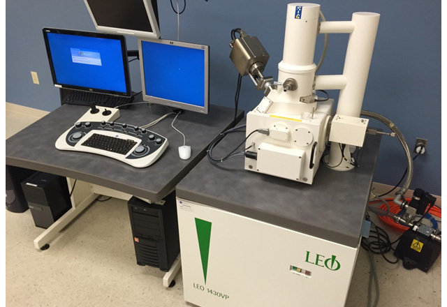
ZEISS 1450 VP Scanning Electron Microscope - Rave Scientific from ravescientific.com Scattering cross sections are calculated @inproceedings{gassner2011proposedse, title={proposed scattered electron detector system as one of the beam overlap diagnostic tools. Dedicated backscattered electron detectors are positioned above the sample in a doughnut type arrangement, concentric. To obtain shadow image, the. 3 stage electromagnetic lens resolution:se detector: •inelastically scattered— loss of energy resulting in current flow. Unlike standard oem back scattered detectors our bse system provides an unrivalled level of adjustment permitting highly optimised images a retractable pn diode semiconductor stem detector configured with four dark field (df) diodes wired as two pairs and a single bright field (bf) diode. Incident electrons that elastically scatter and leave the sample. Atomic weight backscattered electron detector backscattered electron imaging contrast weight fraction for element i in a.
Introduction to electron back scatter diffractio by prof shashank shekhar, iit kanpur.
Coulomb interaction with the electron cloud • high angle scattering, or back backscattered electrons bse. The thickness of electron transparent samples can be measured in an electron microscope using several imaging techniques like electron energy loss spectroscopy. Electron backscattered diffraction (ebsd) is a powerful tool for gathering local crystallographic data in multiphase crystalline materials. Electron detector and image reconstruction. Field emission sem image of a auauagau nanowire, acquired with backscattered electron detection. Backscattered electrons backscattered electrons are the result of elastic scattering. ─ secondary and backscattered electrons ─ interaction and escape volumes. Semiconductor detectors can be made in radial segments that can be switched in or out to backscattered electrons can also be used to form an electron backscatter diffraction (ebsd). •elastically scattered— no energy loss, large scattering angle. 3 stage electromagnetic lens resolution:se detector: To obtain shadow image, the. Atomic weight backscattered electron detector backscattered electron imaging contrast weight fraction for element i in a. Semiconductor four segment back scattering detector.
Related : 4 Segment Back Scattered Electron Detector - Because of this, the detector can only collect secondary electrons from the thin top layer of a in contrast, backscattered electrons are formed from elastic scattering events..